

KL720 Bootstrap config concern

Dear Sir,
I am designing with KL720 269-Ball SOC. I have some wonders regarding to bootstrap configures.
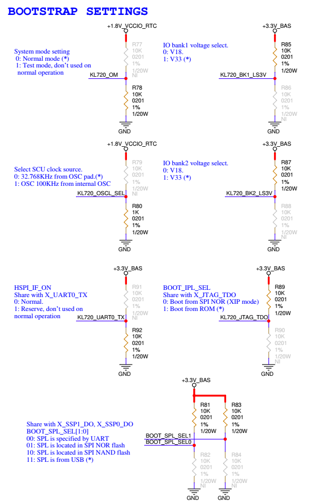
Could you give me more detail about the BOOT_IPL_SEL setting? What is XIP mode? ROM is SPI Nand Flash ex: W25N01GVZEIG, right?
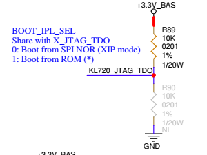
Could you give me more details about the BOOT_SPL_SEL[1:0] setting? If I bring up new board at the first time with a blank/empty SPI flash. could I program Firmware to SPI Flash through USB 3.0 or UART interface with this BOOT_SPL_SEL[1:0] setting?
The discussion has been closed due to inactivity. To continue with the topic, please feel free to post a new discussion.
Comments
Hi,
As you know, there are two boot strap configurations:
In general, we usually use the KL720's ROM as the IPL. For the SPL, we initially use UART and a PC tool (Keil) during development, and then, once the development is successful, we can burn it to NAND flash and select 'boot from SPI NAND'
Thanks Warren.
Could you describe the role of the JTAG interface? Is It needed for bring-up board?
Because we are designing a small device such USB stick, due to the board space so limited and we need to know what is necessary interface for program/debug/bring up board and route them to header/test point. Could we remove the JTAG from below debug header?
Hi Nguyen,
J-Link
J-Link is a family of debugging tools provided by SEGGER Microcontroller, designed to work with JTAG and other debug protocols. J-Link is widely used in the embedded systems industry for debugging and programming microcontrollers from various manufacturers.
Features of J-Link:
here's the link for it:
SEGGER - The Embedded Experts - Downloads - J-Link / J-Trace
I'm not sure about the purpose of the 'USB stick.' However, for programming and debugging, I recommend reserving the UART0/JTAG interface.
If you're concerned about board space, you can reserve just the KL720_JTAG_TMS and KL720_JTAG_TCK pins. J-Link supports SWD (Serial Wire Debug) mode. I've also attached the connection details for J-Link SWD mode for your reference.
HI Warren,
"In general, we usually use the KL720's ROM as the IPL. For the SPL, we initially use UART and a PC tool (Keil) during development, and then, once the development is successful, we can burn it to NAND flash and select 'boot from SPI NAND'"
That means the KL720 IC from the factory has programmed a default ROM that initial common interfaces (UART, USB, JTAG, SPI Flash ) before it has been shipped to the user, right?
In bring-up process, could we burn the FW image to blank NAND FLash through KL720's UART or JTAG or USB interface?
Hi Nguyen,
It's possible to burn the KL720 FW image to blank flash through UART and JTag (JLink), but you need to set the HW setup to change bootstrap to UART mode before burning by UART. The Jlink would be the easier way to access flash.
To use USB to program flash, there should be corresponding FW to handle the USB programming protocol, so it is not available to burn FW image to blank flash through USB.